
Power Device Packaging: Die Attach, Bonding, Moulding and Test
Automated power device packaging in Shenzhen: die attach, wire bonding, moulding, trim and form, 100% electrical test. 50 million units per month capacity.
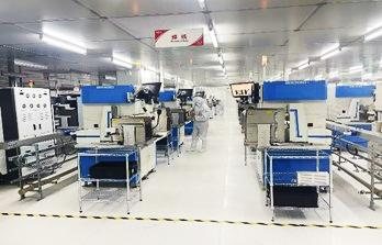
Semiconductor packaging converts a bare die into a solderable, protected, electrically tested device. OCENME runs automated packaging lines in Shenzhen with 50 million units per month capacity, covering die attach, wire bonding, moulding, trim and form and 100% electrical test across TO-220, TO-252, TO-263, TO-247, PDFN and TOLL outlines.
When this process applies
This page covers the assembly and test operations we perform on incoming die: attach, interconnect, encapsulate, singulate and test. Wafer fabrication and wafer-level test sit with our foundry partners. Devices that need a custom lead frame or a non-standard outline are handled as a development project rather than a catalogue part.
Technical specifications
| Packaging capacity | 50 million units per month |
|---|---|
| Plant established | 2021, fully automated lines; equipment expanded in 2024 |
| Die attach | Solder and high-temperature attach, X-ray void inspection on samples |
| Interconnect | Copper wire, aluminium ribbon and clip bonding |
| Encapsulation | Transfer moulding, UL 94V-0 compound, post-mould cure |
| Test | 100% electrical test on final electrical parameters before marking |
| Traceability | ERP, MES and WMS records link wafer lot to shipping carton |
| Outlines | TO-220 series, TO-247, TO-3P, TO-252, TO-251, TO-262, TO-263, PDFN 5×6, PDFN 3×3, TOLL4 |
Where it is the right choice
- Discrete power MOSFETs, diodes and bridges in the outlines listed above
- Devices where die comes from your foundry and you need assembly plus test
- Mature part numbers moving from another assembler, with a documented transfer plan
- Custom marking and packing formats for distribution customers
Where it is the wrong choice
Stating this explicitly matters more than a capability list: if your part falls into one of these categories, another process will cost you less.
- Bare die or wafer-level packaging — we do not offer WLCSP or flip chip
- Modules with insulated substrates (IMS, DBC) — outside our assembly scope
- Automotive-grade parts requiring IATF 16949 process control and PPAP
- Any part where the outline does not exist as a qualified lead frame in our tooling
Equipment
- Automatic dicing and die attach stations
- Copper wire bonders with pull and shear test capability
- Transfer moulding presses with post-mould cure ovens
- Trim, form and singulation tooling per outline
- Automatic test handlers per package family
- Laser marking with lot and date coding
- X-ray inspection (YXLON) and C-SAM (Sonoscan PVA)
Process questions
Can you assemble devices from die we supply?
Yes, subject to die incoming inspection and a documented handling agreement. We inspect for edge chipping and probe marks, record the wafer lot, and confirm the die attach and bond pad metallisation suit our process. We do not accept consigned die without a signed yield and loss allocation, because assembly yield on someone else’s die is a shared risk.
What is the minimum production quantity for a custom packaged part?
It depends on lead frame tooling. On an existing qualified frame, minimum runs are set by line efficiency rather than tooling; on a new frame, the tooling cost dominates and the minimum is a full reel or tube quantity per run. We quote both numbers separately so the tooling amortisation is visible.
How do you prevent mixing lots on an automated line?
Every carrier and magazine carries the lot code, and MES blocks a station from accepting a lot that does not match the work order. Marking is laser applied with date and lot, and outgoing inspection checks the label against the packing list. Mixed lots are the classic failure of semiconductor assembly, so this control is audited, not assumed.
Do you package SiC devices on the same lines as silicon?
SiC runs on the same packaging platform with different die attach and mould compound, and with dedicated consumables where cross-contamination would matter. SiC die are thinner and more brittle, so bond parameters and ejector settings are re-qualified per die type rather than reused from silicon.
Related capabilities and products
Reliability Testing
Reliability testing establishes whether a packaged device survives the thermal, electrical and humidity stress of its application over time. OCENME runs nine test types in-house to JESD22 methods — HTRB, H3TRB, HT/HU, HTSL, temperature cycling, thermal shock, solderability, RSH and HPC — with X-ray, C-SAM and die shear capability for failure analysis..
View capabilityCustom Device Development
Custom device development means defining a part that does not exist in a catalogue: a specific RDS(on) and voltage class, a non-standard outline, or a private marking. OCENME develops custom power devices with foundry die selection, DFN/QFN/TOLL outline qualification and customer-approved marking, with R&D spending of CNY 10 million in 2024..
View capabilityTraceability & Quality System
Traceability is the ability to walk from a device in a customer’s hand back to the wafer lot it came from, and forward from any wafer lot to every carton shipped. OCENME maintains that chain through ERP, MES and WMS records under an ISO 9001:2015 quality system, with lot codes marked on every unit and PCN notification before process or die source changes..
View capabilityKnowledge Base
Tolerance tables, cost mechanics and DFM rules written for buyers rather than engineers.
Read articlesSend the part number and the operating conditions
Tell us the voltage class, current, switching frequency and what the device is replacing. You will get a datasheet, a parameter comparison at matched conditions, and a quotation with MOQ and lead time.