
High Voltage MOSFETs, 400 V to 800 V, Planar and Super Junction
500 V to 700 V N-channel MOSFETs in planar and super junction technology, TO-220F, TO-262F, TO-263 and TO-252. Avalanche rated, ISO 9001:2015 assembly.
A high voltage MOSFET is an N-channel switch rated between 400 V and 800 V, used in offline power supplies where the drain sees rectified mains plus leakage-inductance ringing. OCENME supplies 500 V to 700 V planar MOSFETs and 650 V super junction MOSFETs from 150 mΩ, at continuous drain currents of 7 A to 28 A, in TO-220F, TO-262F, TO-263 and TO-252 packages.
Scope: what this product page covers
This page covers 400 V to 800 V N-channel devices for flyback and forward converters, PFC stages, LLC primary switches, inverter half-bridges and ballast circuits. For 30 V to 200 V switching see the low voltage MOSFET page; for 650 V and 800 V silicon carbide see the SiC MOSFET page.
Specifications
| Voltage class | 500 V, 600 V, 650 V, 700 V; 800 V on request |
|---|---|
| Continuous drain current | 7 A to 28 A at TC = 25 °C |
| On-resistance (typ.) | 150 mΩ at 650 V / 20 A super junction; 0.18 Ω at 500 V / 28 A planar |
| Technology | Planar high voltage; charge-compensated super junction |
| Avalanche | Single-pulse avalanche energy rated; 100% avalanche tested on super junction types |
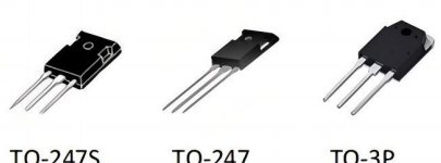
| Packages | TO-220F, TO-220F-2L, TO-262F, TO-263, TO-252, TO-247, TO-3P |
| Gate drive | 10 V characterised; VGS(th) typically 2–4 V |
| Junction temperature | 150 °C maximum; 175 °C on selected super junction types |
Materials
- Silicon die, planar or super junction process, from qualified foundries
- Copper lead frame with isolated full-pack option on TO-220F
- Moulding compound rated UL 94V-0
- Copper wire bonding
Manufacturing process
- Die incoming and dicing Super junction die are inspected for edge chipping before dicing, because charge-balance structures are sensitive to termination damage.
- Die attach Solder die attach with X-ray void inspection on sampled units against an internal void limit.
- Bonding Source and gate bonded; wire pull tested each shift. Super junction types are avalanche tested before packing.
- Moulding Transfer moulding, post-mould cure, and isolation test between tab and pins on TO-220F full-pack parts.
- Test and mark BVDSS, RDS(on), VGS(th) and IDSS tested, plus avalanche where specified, then laser marking with date and lot code.
- Outgoing inspection AQL sampling on marking, lead coplanarity, packing quantity and label against the packing list.
High Voltage & Super Junction MOSFETs in production
Typical applications
- Flyback and forward converters in adapters from 45 W to 300 W
- Active PFC stages in LED drivers, server PSUs and telecom rectifiers
- LLC and half-bridge primary switches
- Inverter stages in welding machines and motor drives
- High-intensity discharge and LED ballast circuits
Quality and documentation
- BVDSS tested at 100% to the datasheet minimum, not sampled
- Avalanche energy tested on super junction types where the datasheet specifies it
- HTRB and H3TRB reports available per part number for high-humidity applications
- Isolation voltage test between tab and pins on TO-220F full-pack parts
- PCN notification before any die source or mould compound change
What we do not do
These are not automotive-qualified parts: we do not hold AEC-Q101 qualification, PPAP capability or IATF 16949 certification for them. We also do not supply 1200 V silicon MOSFETs — above 900 V the practical answer is silicon carbide, and we will say so instead of stretching an 800 V part into a 1000 V application. Designs close to the mains transient limit need a margin review against your surge specification; we quote the margin we can support, not the margin the customer hopes for.
Technical questions
When should I use a super junction MOSFET instead of a planar one?
Super junction wins when conduction loss and die area both matter, typically above 150 W output where the RDS(on) advantage compounds with lower Qg and Coss. Planar parts remain the better choice where avalanche robustness dominates, where cost binds, or where the design is already EMI-marginal and the sharper super junction edge makes it worse.
What voltage margin do I need on a 650 V MOSFET in a 230 V AC design?
Universal input rectifies to about 375 V DC, and flyback leakage-inductance ringing adds 100–200 V on top. A 650 V device therefore leaves roughly 75–175 V of margin, which is why 650 V is the standard class for universal-input adapters. If your clamp is weak or the surge environment is severe, move to 700 V or 800 V rather than tightening the snubber alone.
Are your high voltage MOSFETs avalanche rated?
Super junction types are single-pulse avalanche energy rated and avalanche tested; EAS and IAR appear in each datasheet with the test inductance and starting junction temperature. Avalanche rating is not a licence to run in repetitive avalanche without a thermal calculation.
Can I get samples before committing to a production order?
Yes. Samples ship from stock or from the next packaging lot with the datasheet and a test record. Evaluate at your actual switching frequency and heatsink: a 650 V part that runs cool at 65 kHz can exceed its junction limit at 130 kHz with the same current.
Adjacent products and capabilities
Low & Medium Voltage MOSFETs
A low voltage power MOSFET is an N-channel switching device used below 200 V, where conduction loss dominates and on-resistance decides efficiency. OCENME supplies 30 V to 200 V trench and shielded-gate (SGT) MOSFETs from 1.6 mΩ on-resistance and 220 A continuous drain current, in TO-220, TO-252, TO-263, TO-262 and PDFN 5×6 packages, packaged in Shenzhen at 50 million units per month..
View productSiC MOSFETs
A silicon carbide MOSFET is a wide-bandgap switch that replaces a silicon super junction device at the same voltage while removing most of the body-diode reverse recovery loss. OCENME supplies 650 V and 800 V SiC MOSFETs from 11 A to 20 A in TO-252 and TO-220F, with a 175 °C junction rating, for PFC stages, LLC converters and chargers running above 30 kHz..
View productFast Recovery Diodes
A fast recovery diode is a PN rectifier engineered for short reverse recovery, so it can freewheel in a switching converter without dominating turn-on loss in the opposing switch. OCENME supplies fast recovery diodes from 200 V to 1500 V in TO-220, TO-247, TO-3P, TO-252 and TO-263 packages, with Trr and IFSM stated per ordering code in the datasheet..
View productQuality & Inspection
CMM inspection to ±0.002 mm, FAI reports and PPAP documentation for every order.
Inspection capabilitySend the part number and the operating conditions
Tell us the voltage class, current, switching frequency and what the device is replacing. You will get a datasheet, a parameter comparison at matched conditions, and a quotation with MOQ and lead time.