
Low and Medium Voltage Power MOSFETs, 30 V to 200 V
N-channel power MOSFETs from 30 V to 200 V in TO-220, TO-252, TO-263 and PDFN packages. On-resistance from 1.6 mΩ, 220 A rating, ISO 9001:2015 packaging.
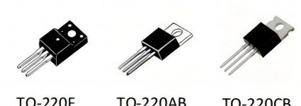
A low voltage power MOSFET is an N-channel switching device used below 200 V, where conduction loss dominates and on-resistance decides efficiency. OCENME supplies 30 V to 200 V trench and shielded-gate (SGT) MOSFETs from 1.6 mΩ on-resistance and 220 A continuous drain current, in TO-220, TO-252, TO-263, TO-262 and PDFN 5×6 packages, packaged in Shenzhen at 50 million units per month.
Scope: what this product page covers
This page covers N-channel devices from 30 V to 200 V used as synchronous rectifiers, load switches, battery-protection switches, DC/DC low-side and high-side switches and motor drive stages up to 200 V. Above 200 V the switching loss and avalanche behaviour change enough that the high voltage MOSFET page is the better starting point.
Specifications
| Voltage class | 30 V, 40 V, 60 V, 80 V, 85 V, 100 V, 200 V |
|---|---|
| Continuous drain current | 9 A to 220 A at TC = 25 °C |
| On-resistance (typ.) | 1.6 mΩ at 60 V / 220 A; 3.0 mΩ at 30 V / 100 A |
| Gate drive | 4.5 V and 10 V characterised; logic-level options |
| Packages | TO-220, TO-220F, TO-252, TO-263, TO-262F, PDFN 5×6, PDFN 3×3, TOLL |
| Channel | N-channel enhancement mode; P-channel on request |
| Junction temperature | 150 °C maximum on most types; 175 °C on selected SGT types |
| Packaging capacity | 50 million units per month on automated lines |
Materials
- Silicon die from qualified foundries, trench and SGT process
- Copper lead frame with matte tin plating
- Moulding compound rated UL 94V-0
- Solder die attach; copper wire and aluminium ribbon bonding
Manufacturing process
- Incoming die inspection Wafer-level visual and electrical sampling before dicing; the foundry wafer lot is recorded against the assembly lot.
- Dicing and die attach Wafer mounted and diced, then die attached to the copper lead frame with solder; voiding checked by X-ray on sampled units.
- Wire bonding Source and gate bonded with copper wire or aluminium ribbon; wire pull and die shear tested each shift against JESD22 methods.
- Moulding and cure Epoxy moulding to the package outline, post-mould cure, then deflash and plating.
- Trim, form and test Leads trimmed to the package drawing; every unit electrically tested for VGS(th), RDS(on), leakage and breakdown before marking.
- Marking and packing Laser marking with lot code, tape-and-reel or tube packing, outgoing inspection on AQL sampling.
Low & Medium Voltage MOSFETs in production
Typical applications
- Synchronous rectification in AC/DC adapters and chargers
- DC/DC converters in telecom, server and industrial power
- Battery protection and load switching in power tools and light EVs
- Motor drive stages in fans, pumps and small inverters
- ORing and hot-swap circuits in redundant power systems
Quality and documentation
- 100% electrical test on RDS(on), VGS(th), IDSS and BVDSS before marking
- Lot-level traceability from foundry wafer lot to shipping carton through ERP and MES records
- Reliability screening available: HTRB, H3TRB, temperature cycling, thermal shock, solderability
- Datasheet with full absolute maximum ratings and characterised curves supplied per ordering code
- ISO 9001:2015 quality system; certificate copy and scope available on request
What we do not do
We do not manufacture wafers. Die are sourced from qualified foundries and assembled in our own packaging plant, so wafer-level process changes are governed by the foundry, not by us — we notify customers of die source changes under our PCN process. We do not claim AEC-Q101 qualification, PPAP submission or IATF 16949 certification for these parts, and we do not supply automotive-grade devices. For 48 V systems above 100 A continuous, the package and heatsink limit the rating before the die does, so we run a thermal review before quoting.
Technical questions
What is the difference between trench and SGT MOSFETs?
Trench MOSFETs use a vertical gate trench to raise channel density; SGT (shielded gate trench) adds a source-connected shield electrode below the gate, which cuts gate charge and switch-node ringing. At the same RDS(on), an SGT part shows lower Qg, which is why SGT dominates 30–100 V synchronous rectification. We supply both and quote whichever your efficiency target requires.
Can you supply a drop-in replacement for a MOSFET I already use?
Send the full part number, package and operating conditions — switching frequency, gate drive voltage, current waveform and heatsinking. We compare voltage class, RDS(on) at your gate voltage, Qg, Coss and the body diode, then quote only where the comparison holds. A voltage and current rating alone is not enough to confirm a replacement.
What is the minimum order quantity for power MOSFETs?
MOQ is set per ordering code and packing format, because a tape-and-reel quantity differs from a tube quantity, and it is confirmed in the quotation rather than published as a blanket number. Sample quantities for evaluation are available before a production order.
Do you provide reliability test reports with the shipment?
A certificate of conformance and the electrical test record accompany each lot. Reliability reports — HTRB, H3TRB, temperature cycling, thermal shock — are supplied per part number on request, with test conditions and sample size stated. They are lot-specific reports, not generic marketing documents.
Adjacent products and capabilities
High Voltage & Super Junction MOSFETs
A high voltage MOSFET is an N-channel switch rated between 400 V and 800 V, used in offline power supplies where the drain sees rectified mains plus leakage-inductance ringing. OCENME supplies 500 V to 700 V planar MOSFETs and 650 V super junction MOSFETs from 150 mΩ, at continuous drain currents of 7 A to 28 A, in TO-220F, TO-262F, TO-263 and TO-252 packages..
View productSiC MOSFETs
A silicon carbide MOSFET is a wide-bandgap switch that replaces a silicon super junction device at the same voltage while removing most of the body-diode reverse recovery loss. OCENME supplies 650 V and 800 V SiC MOSFETs from 11 A to 20 A in TO-252 and TO-220F, with a 175 °C junction rating, for PFC stages, LLC converters and chargers running above 30 kHz..
View productSiC Schottky Diodes
A SiC Schottky barrier diode is a majority-carrier rectifier with no minority-carrier reverse recovery, used where a silicon fast recovery diode would waste switching energy. OCENME supplies a 650 V, 20 A SiC Schottky family with 1.34 V forward drop, 130 A surge current and a 175 °C junction rating, in TO-220AC, TO-220FAC and TO-247 outlines..
View productQuality & Inspection
CMM inspection to ±0.002 mm, FAI reports and PPAP documentation for every order.
Inspection capabilitySend the part number and the operating conditions
Tell us the voltage class, current, switching frequency and what the device is replacing. You will get a datasheet, a parameter comparison at matched conditions, and a quotation with MOQ and lead time.