
Silicon Carbide MOSFETs, 650 V and 800 V
Silicon carbide N-channel MOSFETs at 650 V and 800 V, 11 A to 20 A, in TO-220F and TO-252. Low Qrr, 175 °C junction rating, ISO 9001:2015 assembly.
A silicon carbide MOSFET is a wide-bandgap switch that replaces a silicon super junction device at the same voltage while removing most of the body-diode reverse recovery loss. OCENME supplies 650 V and 800 V SiC MOSFETs from 11 A to 20 A in TO-252 and TO-220F, with a 175 °C junction rating, for PFC stages, LLC converters and chargers running above 30 kHz.
Scope: what this product page covers
This page covers 650 V and 800 V N-channel SiC MOSFETs for hard-switched PFC, LLC primary side, on-board chargers, solar micro-inverters and high-frequency DC/DC. SiC Schottky diodes have their own page; 1200 V SiC devices are not in the current datasheet set.
Specifications
| Voltage class | 650 V and 800 V |
|---|---|
| Continuous drain current | 11 A to 20 A at TC = 25 °C |
| On-resistance (typ.) | 154 mΩ at 800 V / 15 A, VGS = 18 V, TC = 25 °C |
| Gate drive | On-resistance specified at 15–18 V; 18 V is the recommended maximum |
| Junction temperature | 175 °C maximum |
| Body diode | Low reverse recovery charge; rugged against parasitic turn-on at 0 V gate |
| Packages | TO-252 (DPAK), TO-220F |
| Die source | Wide-bandgap SiC die from qualified foundries, assembled in Shenzhen |
Materials
- Silicon carbide (4H-SiC) die from qualified foundries
- Copper lead frame with matte tin plating
- High-temperature moulding compound rated UL 94V-0
- Sintered or high-temperature solder die attach for 175 °C operation
Manufacturing process
- Die incoming SiC die are accepted against the foundry gate-oxide screening data; the foundry wafer lot is recorded against the assembly lot.
- Die attach High-temperature die attach selected for 175 °C operation, with X-ray void inspection on sampled units.
- Bonding Gate and source bonded with copper wire; wire pull and die shear monitored each shift, because SiC die are thinner and more brittle than silicon equivalents.
- Moulding High-temperature mould compound, post-mould cure, then isolation test.
- Test VGS(th), RDS(on) at 15 V and 18 V, BVDSS, IDSS and gate leakage tested at 100%, then marked.
- Reliability screening HTRB and H3TRB available as screening or qualification batches, with results reported per lot and test conditions stated.
SiC MOSFETs in production
Typical applications
- Continuous conduction mode PFC above 30 kHz
- LLC and phase-shifted full bridge primary switches
- On-board chargers and DC/DC converters in light EVs
- Solar string inverters and micro-inverters
- Server and telecom rectifiers with high power density targets
Quality and documentation
- 100% electrical test including gate leakage and RDS(on) at two gate voltages
- HTRB and H3TRB reports available per part number
- 175 °C junction rating verified by high-temperature gate bias and storage tests
- Die source and gate-oxide screening data traceable to the foundry lot
- Gate drive application note supplied with first orders
What we do not do
We are not a SiC wafer fab and we do not claim a proprietary SiC process — die come from qualified foundries and we package and test them. We do not hold AEC-Q101 qualification or automotive-grade status for these devices, and 1200 V SiC parts are not listed. SiC MOSFETs are sensitive to gate-loop inductance and negative gate transients; driven from a silicon MOSFET gate driver with no negative-bias review, they fail for reasons that are not the device’s fault. We ask for the gate drive schematic before quoting.
Technical questions
What gate voltage should I use to drive a SiC MOSFET?
Turn on at 15 V to 18 V, with 18 V the maximum recommended in our datasheets, and bias turn-off to a negative rail, commonly −3 V to −5 V. RDS(on) figures are specified at a stated gate voltage — reading a 154 mΩ value as achievable at 10 V gate drive is a common and expensive mistake.
Do SiC MOSFETs remove the need for a SiC Schottky diode?
In continuous conduction mode PFC the body diode usually suffices, because it conducts only during dead time. In bridgeless or totem-pole PFC the body diode carries real current, so its forward drop and recovery still matter and a discrete SiC Schottky is commonly paralleled. We supply both, so the choice is made on loss numbers rather than supplier convenience.
Why does my SiC MOSFET fail at turn-off when the current is well below rating?
Almost always gate-loop or common-source inductance. A SiC die switches in tens of nanoseconds, so 10 nH of common-source inductance produces a gate spike large enough to turn the device partly back on. The fix is a Kelvin source connection, a tight gate loop and a negative turn-off bias — not a larger device.
Are your SiC parts available in TOLL or PDFN packages?
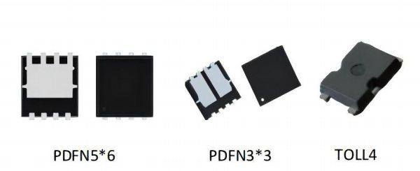
The current datasheet set covers TO-252 and TO-220F. Our plant qualifies TOLL4 and PDFN 5×6 for silicon devices; SiC in those packages is a development question rather than a catalogue item. Ask with your volume and target date and we answer with a real schedule.
Adjacent products and capabilities
Low & Medium Voltage MOSFETs
A low voltage power MOSFET is an N-channel switching device used below 200 V, where conduction loss dominates and on-resistance decides efficiency. OCENME supplies 30 V to 200 V trench and shielded-gate (SGT) MOSFETs from 1.6 mΩ on-resistance and 220 A continuous drain current, in TO-220, TO-252, TO-263, TO-262 and PDFN 5×6 packages, packaged in Shenzhen at 50 million units per month..
View productHigh Voltage & Super Junction MOSFETs
A high voltage MOSFET is an N-channel switch rated between 400 V and 800 V, used in offline power supplies where the drain sees rectified mains plus leakage-inductance ringing. OCENME supplies 500 V to 700 V planar MOSFETs and 650 V super junction MOSFETs from 150 mΩ, at continuous drain currents of 7 A to 28 A, in TO-220F, TO-262F, TO-263 and TO-252 packages..
View productSiC Schottky Diodes
A SiC Schottky barrier diode is a majority-carrier rectifier with no minority-carrier reverse recovery, used where a silicon fast recovery diode would waste switching energy. OCENME supplies a 650 V, 20 A SiC Schottky family with 1.34 V forward drop, 130 A surge current and a 175 °C junction rating, in TO-220AC, TO-220FAC and TO-247 outlines..
View productQuality & Inspection
CMM inspection to ±0.002 mm, FAI reports and PPAP documentation for every order.
Inspection capabilitySend the part number and the operating conditions
Tell us the voltage class, current, switching frequency and what the device is replacing. You will get a datasheet, a parameter comparison at matched conditions, and a quotation with MOQ and lead time.